
PRODUCTS AND SPECIFICATIONS DISCUSSED HEREIN ARE SUBJECT TO CHANGE BY MICRON WITHOUT NOTICE.
1
256Mb: x4, x8, x16 SDRAM
Micron Technology, Inc., reserves the right to change products or specifications without notice.
256MSDRAM_F.p65 ≠ Rev. F; Pub. 1/03
©2003, Micron Technology, Inc.
256Mb: x4, x8, x16
SDRAM
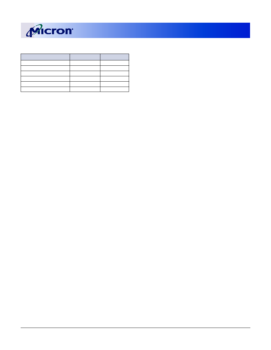
KEY TIMING PARAMETERS
SPEED
CLOCK
ACCESS TIME
SETUP
HOLD
GRADE
FREQUENCY CL = 2* CL = 3*
TIME
TIME
-7E
143 MHz
≠
5.4ns
1.5ns
0.8ns
-75
133 MHz
≠
5.4ns
1.5ns
0.8ns
-7E
133 MHz
5.4ns
≠
1.5ns
0.8ns
-75
100 MHz
6ns
≠
1.5ns
0.8ns
64 Meg x 4
32 Meg x 8
16 Meg x 16
Configuration
16 Meg x 4 x 4 banks 8 Meg x 8 x 4 banks 4 Meg x 16 x 4 banks
Refresh Count
8K
8K
8K
Row Addressing
8K (A0≠A12)
8K (A0≠A12)
8K (A0≠A12)
Bank Addressing
4 (BA0, BA1)
4 (BA0, BA1)
4 (BA0, BA1)
Column Addressing
2K (A0≠A9, A11)
1K (A0≠A9)
512 (A0≠A8)
SYNCHRONOUS
DRAM
MT48LC64M4A2 ≠ 16 Meg x 4
x 4 banks
MT48LC32M8A2 ≠ 8 Meg x 8
x 4 banks
MT48LC16M16A2 ≠ 4 Meg x 16 x 4 banks
For the latest data sheet, please refer to the Micron Web site:
www.micron.com/dramds
PIN ASSIGNMENT (Top View)
54-Pin TSOP
FEATURES
∑ PC66-, PC100-, and PC133-compliant
∑ Fully synchronous; all signals registered on
positive edge of system clock
∑ Internal pipelined operation; column address can
be changed every clock cycle
∑ Internal banks for hiding row access/precharge
∑ Programmable burst lengths: 1, 2, 4, 8, or full page
∑ Auto Precharge, includes CONCURRENT AUTO
PRECHARGE, and Auto Refresh Modes
∑ Self Refresh Mode
∑ 64ms, 8,192-cycle refresh
∑ LVTTL-compatible inputs and outputs
∑ Single +3.3V ±0.3V power supply
OPTIONS
MARKING
∑ Configurations
64 Meg x 4
(16 Meg x 4
x 4 banks)
64M4
32 Meg x 8
( 8 Meg x 8
x 4 banks)
32M8
16 Meg x 16 ( 4 Meg x 16 x 4 banks)
16M16
∑ WRITE Recovery (
t
WR)
t
WR = "2 CLK"
1
A2
∑ Package/Pinout
54-pin TSOP II OCPL
2
(400 mil)
TG
60-ball FBGA (8mm x 16mm) (x4, x8)
FB
4, 5
54-ball FBGA (8mm x 14mm) (x16 only)
FG
3
∑ Timing (Cycle Time)
7.5ns @ CL = 2 (PC133)
-7E
7.5ns @ CL = 3 (PC133)
-75
∑ Self Refresh
Standard
None
Low power
L
3
∑ Operating Temperature
Commercial (0
o
C to +70
o
C)
None
Industrial (-40
o
C to +85
o
C)
IT
3
NOTE: 1. Refer to Micron Technical Note TN-48-05.
2. Off-center parting line.
3. Consult Micron for availability.
4. Not available in x16 configuration.
5. Actual FBGA part marking shown on page 60.
Part Number Example:
MT48LC16M16A2TG-75
Note:
The # symbol indicates signal is active LOW. A dash (≠)
indicates x8 and x4 pin function is same as x16 pin function.
V
DD
DQ0
V
DD
Q
DQ1
DQ2
VssQ
DQ3
DQ4
V
DD
Q
DQ5
DQ6
VssQ
DQ7
V
DD
DQML
WE#
CAS#
RAS#
CS#
BA0
BA1
A10
A0
A1
A2
A3
V
DD
1
2
3
4
5
6
7
8
9
10
11
12
13
14
15
16
17
18
19
20
21
22
23
24
25
26
27
54
53
52
51
50
49
48
47
46
45
44
43
42
41
40
39
38
37
36
35
34
33
32
31
30
29
28
Vss
DQ15
VssQ
DQ14
DQ13
V
DD
Q
DQ12
DQ11
VssQ
DQ10
DQ9
V
DD
Q
DQ8
Vss
NC
DQMH
CLK
CKE
A12
A11
A9
A8
A7
A6
A5
A4
Vss
x8
x16
x16
x8
x4
x4
-
DQ0
-
NC
DQ1
-
NC
DQ2
-
NC
DQ3
-
NC
-
NC
-
-
-
-
-
-
-
-
-
-
-
-
-
NC
-
NC
DQ0
-
NC
NC
-
NC
DQ1
-
NC
-
NC
-
-
-
-
-
-
-
-
-
-
-
-
-
DQ7
-
NC
DQ6
-
NC
DQ5
-
NC
DQ4
-
NC
-
-
DQM
-
-
-
-
-
-
-
-
-
-
-
-
NC
-
NC
DQ3
-
NC
NC
-
NC
DQ2
-
NC
-
-
DQM
-
-
-
-
-
-
-
-
-
-
-
*CL = CAS (READ) latency

2
256Mb: x4, x8, x16 SDRAM
Micron Technology, Inc., reserves the right to change products or specifications without notice.
256MSDRAM_F.p65 ≠ Rev. F; Pub. 1/03
©2003, Micron Technology, Inc.
256Mb: x4, x8, x16
SDRAM
60-BALL FBGA ASSIGNMENT
(Top View)
64 Meg x 4 SDRAM
8mm x 16mm "FB"
32 Meg x 8 SDRAM
8mm x 16mm "FB"
NOTE: FBGA pin Symbol, Type, and Descriptions are identical to the listing of the 54-pin TSOP table on page 9.
A
B
C
D
E
F
G
H
J
K
L
M
N
P
R
1
2
3
4
5
6
7
8
Depopulated Balls
NC
Vss
NC
VssQ
V
DD
Q
DQ3
NC
NC
NC
VssQ
V
DD
Q
DQ2
NC
NC
NC
Vss
NC
DQM
NC
CK
A12
CKE
A11
A9
A8
A7
A6
A5
A4
Vss
V
DD
NC
V
DD
Q
NC
DQ0
VssQ
NC
NC
V
DD
Q
NC
DQ1
VssQ
NC
NC
V
DD
NC
WE#
CAS#
RAS#
NC
NC
CS#
BA1
BA0
A0
A10
A2
A1
V
DD
A3
A
B
C
D
E
F
G
H
J
K
L
M
N
P
R
1
2
3
4
5
6
7
8
Depopulated Balls
DQ7
Vss
NC
VssQ
V
DD
Q
DQ6
DQ5
NC
NC
VssQ
V
DD
Q
DQ4
NC
NC
NC
Vss
NC
DQM
NC
CK
A12
CKE
A11
A9
A8
A7
A6
A5
A4
Vss
V
DD
DQ0
V
DD
Q
NC
DQ1
VssQ
NC
DQ2
V
DD
Q
NC
DQ3
VssQ
NC
NC
V
DD
NC
WE#
CAS#
RAS#
NC
NC
CS#
BA1
BA0
A0
A10
A2
A1
V
DD
A3

3
256Mb: x4, x8, x16 SDRAM
Micron Technology, Inc., reserves the right to change products or specifications without notice.
256MSDRAM_F.p65 ≠ Rev. F; Pub. 1/03
©2003, Micron Technology, Inc.
256Mb: x4, x8, x16
SDRAM
54-BALL VFBGA ASSIGNMENT
(Top View)
16 Meg x 16 SDRAM
8mm x 14mm "FG"
A
B
C
D
E
F
G
H
J
1
2
3
4
5
6
7
8
9
Depopulated Balls
Vss
DQ15
DQ14
DQ13
DQ12
DQ11
DQ10
DQ9
DQ8
NC
UDQM
CLK
A12
A11
A8
A7
Vss
A5
V
SS
Q
V
DD
Q
V
SS
Q
V
DD
Q
Vss
CKE
A9
A6
A4
V
DD
Q
VssQ
V
DD
Q
V
SS
Q
V
DD
CAS#
BA0
A0
A3
DQ0
V
DD
DQ2
DQ1
DQ4
DQ3
DQ6
DQ5
LDQM
DQ7
RAS#
WE#
BA1
CS#
A1
A10
A2
V
DD
4
256Mb: x4, x8, x16 SDRAM
Micron Technology, Inc., reserves the right to change products or specifications without notice.
256MSDRAM_F.p65 ≠ Rev. F; Pub. 1/03
©2003, Micron Technology, Inc.
256Mb: x4, x8, x16
SDRAM
GENERAL DESCRIPTION
The 256Mb SDRAM is a high-speed CMOS,
dynamic random-access memory containing
268,435,456 bits. It is internally configured as a quad-
bank DRAM with a synchronous interface (all signals
are registered on the positive edge of the clock signal,
CLK). Each of the x4's 67,108,864-bit banks is orga-
nized as 8,192 rows by 2,048 columns by
4 bits. Each of the x8's 67,108,864-bit banks is orga-
nized as 8,192 rows by 1,024 columns by 8 bits. Each of
the x16's 67,108,864-bit banks is organized as 8,192
rows by 512 columns by 16 bits.
Read and write accesses to the SDRAM are burst
oriented; accesses start at a selected location and con-
tinue for a programmed number of locations in a pro-
grammed sequence. Accesses begin with the registra-
tion of an ACTIVE command, which is then followed by
a READ or WRITE command. The address bits regis-
tered coincident with the ACTIVE command are used
PART NUMBER ARCHITECTURE PACKAGE
MT48LC64M4A2TG
64 Meg x 4
54-pin TSOP II
MT48LC64M4A2FB*
64 Meg x 4
60-ball FBGA
MT48LC32M8A2TG
32 Meg x 8 54-pin TSOP II
MT48LC32M8A2FB*
32 Meg x 8 60-ball FBGA
MT48LC16M16A2TG
16 Meg x 16 54-pin TSOP II
MT48LC16M16A2FG
16 Meg x 16 54-ball FBGA
*Actual FBGA part marking shown on page 60.
256 Mb SDRAM PART NUMBERS
to select the bank and row to be accessed (BA0, BA1
select the bank; A0≠A12 select the row). The address
bits registered coincident with the READ or WRITE com-
mand are used to select the starting column location
for the burst access.
The SDRAM provides for programmable READ or
WRITE burst lengths of 1, 2, 4, or 8 locations, or the full
page, with a burst terminate option. An auto precharge
function may be enabled to provide a self-timed row
precharge that is initiated at the end of the burst se-
quence.
The 256Mb SDRAM uses an internal pipelined ar-
chitecture to achieve high-speed operation. This ar-
chitecture is compatible with the 2n rule of prefetch
architectures, but it also allows the column address to
be changed on every clock cycle to achieve a high-
speed, fully random access. Precharging one bank
while accessing one of the other three banks will hide
the precharge cycles and provide seamless, high-
speed, random-access operation.
The 256Mb SDRAM is designed to operate in 3.3V
memory systems. An auto refresh mode is provided,
along with a power-saving, power-down mode. All in-
puts and outputs are LVTTL-compatible.
SDRAMs offer substantial advances in DRAM oper-
ating performance, including the ability to synchro-
nously burst data at a high data rate with automatic
column-address generation, the ability to interleave
between internal banks to hide precharge time and
the capability to randomly change column addresses
on each clock cycle during a burst access.

5
256Mb: x4, x8, x16 SDRAM
Micron Technology, Inc., reserves the right to change products or specifications without notice.
256MSDRAM_F.p65 ≠ Rev. F; Pub. 1/03
©2003, Micron Technology, Inc.
256Mb: x4, x8, x16
SDRAM
TABLE OF CONTENTS
Functional Block Diagram ≠ 64 Meg x 4 ....................
6
Functional Block Diagram ≠ 32 Meg x 8 ....................
7
Functional Block Diagram ≠ 16 Meg x 16 ..................
8
Pin Descriptions .......................................................... 10
Ball Descriptions .......................................................... 10
Functional Description ............................................... 12
Initialization ........................................................... 12
Register Definition ................................................ 12
Mode Register ................................................... 12
Burst Length ................................................ 12
Burst Type ................................................... 13
CAS Latency ................................................ 14
Operating Mode .......................................... 14
Write Burst Mode ........................................ 14
Commands ................................................................... 15
Truth Table 1 (Commands and DQM Operation)
.............. 15
Command Inhibit .................................................. 16
No Operation (NOP) .............................................. 16
Load mode register ................................................ 16
Active ....................................................................... 16
Read ....................................................................... 16
Write ....................................................................... 16
Precharge ................................................................ 16
Auto Precharge ....................................................... 16
Burst Terminate ..................................................... 17
Auto Refresh ........................................................... 17
Self Refresh ............................................................. 17
Operation ..................................................................... 18
Bank/Row Activation ............................................. 18
Reads ....................................................................... 19
Writes ....................................................................... 25
Precharge ................................................................ 27
Power-Down ........................................................... 27
Clock Suspend ........................................................ 28
Burst Read/Single Write ....................................... 28
Concurrent Auto Precharge ................................. 29
Truth Table 2 (CKE)
...................................................... 31
Truth Table 3 (Current State, Same Bank)
........................ 32
Truth Table 4 (Current State, Different Bank)
.................. 34
Absolute Maximum Ratings ....................................... 36
DC Electrical Characteristics
and Operating Conditions ....................................... 36
I
DD
Specifications and Conditions ............................. 36
Capacitance .................................................................. 37
Electrical Characteristics
and Recommended AC Operating Conditions ....... 37
AC Electrical Characteristics (Timing Table) ......... 38
Timing Waveforms
Initialize and Load mode register ........................ 40
Power-Down Mode ................................................ 41
Clock Suspend Mode ............................................ 42
Auto Refresh Mode ................................................ 43
Self Refresh Mode .................................................. 44
Reads
Read ≠ Without Auto Precharge ..................... 45
Read ≠ With Auto Precharge ........................... 46
Single Read ≠ Without Auto Precharge ......... 47
Single Read ≠ With Auto Precharge ............... 48
Alternating Bank Read Accesses .................... 49
Read ≠ Full-Page Burst .................................... 50
Read ≠ DQM Operation ................................... 51
Writes
Write ≠ Without Auto Precharge ..................... 52
Write ≠ With Auto Precharge ........................... 53
Single Write - Without Auto Precharge ......... 54
Single Write - With Auto Precharge ................ 55
Alternating Bank Write Accesses ................... 56
Write ≠ Full-Page Burst .................................... 57
Write ≠ DQM Operation ................................... 58